In some of my recent boards, which I will hopefully blog about soon, I decided to add some DRC-violating sections to test how well they would come out. OSH Park has pretty good tolerances — 5/5 trace/space with 10 mil holes and 4 mil annular rings, for their 4-layer boards — but they’re not *quite* good enough to support 0.8mm-pitch BGAs. You can fit one of their vias in between the BGA pads, but you can’t end up routing a trace between two 0.8mm-pitch vias. It’s very close to working — one only needs 4.5/4.5-mil trace/space in order to get it to work. I asked one of the support people at oshpark.com what they suggested, and they said that they’ve seen people have luck violating the trace/space rules, and said to not try violating the via rules (it’s not like they’ll somehow magically make a smaller hole — makes sense). I had a tiny bit of extra room in some recent boards so I decided to put this to the test, before incorporating this into my designs. I took some pictures using a cheap USB microscope that I bought.
My first test was to use a comb-shaped polygon fill. The comb consists of 4 triangles, which go from a point (0-mil “width”) to an 8-mil width. The goal was to test how small the feature size could be. I put some silkscreen on it to mark where the triangles had 0/2/4/6/8-mil width. Here’s what I got (click to enlarge):

You can see that they were able to produce what are supposed to be 2-mil traces and 2-mil spaces, but beyond that the traces disappear or the triangles become solid. I don’t really have a way of measuring if they actually made them to these dimensions, but they seem like they’re approximately the size they should be.
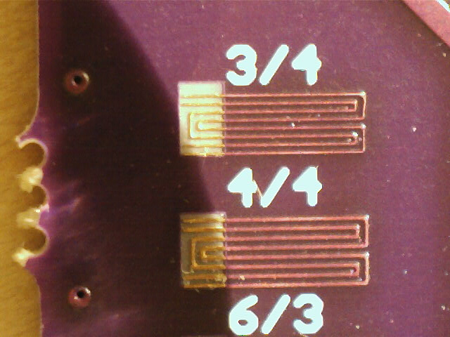
Just because the minimum feature size is potentially 2mil doesn’t mean that you can use that reliably in your designs. I came up with a sub-DRC test pattern, and ran it against a number of different trace/space combinations. Here are some results for 4/4 and 6/3:

In the both pictures, the 4/4 looks surprisingly good. The 6/3 looks like it’s pushing it on the spacing, but electrically these simple test patterns seem to have come out ok (the two separate nets are continuous and not connected to each other). That doesn’t mean I trust that I could use 6/3 for an entire board, and I doubt I’ll ever try it at all, but it’s cool to see that they can do it.
One interesting thing to note is the problems with the silkscreen in the first “4” in “4/4”. Interestingly, the problem is exactly the same in all three boards. You can see a similar problem with the bottom of the “6” and “3”, but I feel like that’s reasonable since I have exposed copper traces right there and the board house presumably clipped that on purpose. I don’t understand why the “4” got the same treatment, though.
Here are some tests that worked out slightly less well:


The 3-mil traces did not survive, and ended up delaminating in all three boards. You can see though just how good the 5/5 traces look in comparison.
Luckily, on a separate set of boards I had also included this same test pattern, but in this case mostly covered with silkscreen. These actually seem to have worked out just fine:
I doubt that I’d ever feel comfortable going this small — a small test pattern on a single run of boards doesn’t prove anything. But seeing how well these turned out makes me feel much more comfortable using 4.5/4.5 trace/space for 0.8mm-pitch BGA fan-out, especially if I can keep the DRC violations on the outer layers where they can be visually inspected.
0.8mm-pitch BGAs would still be quite difficult to do on a 4-layer board, for any decent grid size. If it’s small or not a full grid it’s easier — I was able to route a 0.5mm-pitch BGA on OSH Park’s 2-layer process, since it was a 56-ball BGA formatted as two concentric rings. It’s also not too difficult to route an 0.8mm-pitch BGA DRAM chip, since the balls again are fairly sparse.
I’m looking at some 256-ball 0.8mm-pitch BGAs for FPGAs or processors, which may or may not be possible right now. These tests show me that there’s at least in the realm of possibility, but it might only be practical if there are a large number of unused IO balls.
In my conversation with OSH Park, though, they said they want to start doing 6-layer boards eventually, which are likely to come with another tolerance improvement. I told them to count me in 🙂
Update: wow, wordpress really made a mess of those images. Sorry about that.

5 responses to “Playing with OSH Park tolerances”
Glad someone did this! I was about to order my first fab but might go down to 4.5/4.5 from my usual 5/5 – Thanks pal 🙂
LikeLike
Hey, love the testing you did here. Great work. I’ve been using OSHPark for some time now, for my hobbies, and I’ve started using it for work for fairly cheap prototyping. I’ve been having problems with fairly dense 4 layer boards, in that I’m finding a number of connections shorted together at times, some broken traces, etc. I was using 6 mil traces with 5 mil spacing, and I’m wondering if you recommend continuing at this tolerance, or have any tips to guarantee better fabrication. I have talked with OSH about it, and as per their suggestion, adding a pour to the top and bottom layers around isolated traces has helped. But it’s still not perfect.
Do you have any tips? Additionally, what would you say is your scrap rate with boards you get from them?
LikeLike
Oh interesting — I don’t think I’ve ever had a bad board from them, so I’m not sure how much help I can be here. I use 5/5 regularly, so I’m surprised that you have issues especially given that 6/5 is within the design rules. Do they give a refund when something like that happens?
LikeLike
Is this the 4-layer service or 2-layer?
LikeLike
This is a design i made for the 0.8mm pitch Max10 FPGA. Rather than shrink the tracks, I stayed with 5 mil, and reduced the pads to 0.42mm.
The min spec 18/10 mil vias fit fine in the middle of each square of 4 fpga pads
http://forums.parallax.com/discussion/160368/towards-a-p1v-smorgasboard/p1
LikeLike