This is part 6 of my Building a Processor series, where I try to build a processor on an FPGA board. This post is about optimizing part of the circuit that I built in the previous part.
Previous: simple counter.
In the previous post, I briefly touched on a simple speed optimization that I made to the debouncer circuit, to deal with the fact that the button inputs and sseg outputs are on opposite sides of the fpga. In this post, I’ll talk about area-optimizing the debouncer, since I happen to know that it’s quite inefficient in that regard.
Early optimization caveat
Quick aside before we begin: ISE, and I would assume most EDA tools, optimize your circuit to meet certain constraints. A simple constraint is that your design must fit on the chip you’re targeting, or that you can’t map different logic elements to the same physical element, etc. There are also timing constraints, the main one in the current design being that every path between two clocked registers must have a total delay less than the period of the clock. (ISE refers to this as a PERIOD constraint; there are others that you can add too.) One important thing to know, though, is that the optimizers in ISE will put in different amounts of effort depending on the difficulty of meeting the constraints. In the current design, we’re only using 1% of the FPGA, and the worst-case delay is around 5ns, when the clock period is 100ns. This means that the optimizers will quickly find a placement that meets the constraints, and return. (Note: there are a bunch of options that you can set to tell the optimizers how hard to work, but I found that setting the tools to “optimizing timing performance” mode actually made the timing performance worse for this particular design.) This is good in that the runtime of the synthesis is reasonable, but it means that the area and timing results are the result of minimal effort from the optimizers, and aren’t necessarily reflective of what the tools are capable of producing. For example, here is part of the original timing report:
================================================================================
Timing constraint: TS_dcm_clkfx = PERIOD TIMEGRP "dcm_clkfx" TS_sys_clk_pin *
0.1 HIGH 50%;
For more information, see Period Analysis in the Timing Closure User Guide (UG612).

 1334 paths analyzed, 330 endpoints analyzed, 0 failing endpoints
 0 timing errors detected. (0 setup errors, 0 hold errors, 0 component switching limit errors)
 Minimum period is   4.808ns.
--------------------------------------------------------------------------------

Paths for end point ctr_1 (SLICE_X30Y13.SR), 2 paths
--------------------------------------------------------------------------------
Slack (setup path):     95.192ns (requirement - (data path - clock path skew + uncertainty))
  Source:               debounce_btn[2].btn_db/out (FF)
  Destination:          ctr_1 (FF)
  Requirement:          100.000ns
  Data Path Delay:      3.694ns (Levels of Logic = 1)
  Clock Path Skew:      0.021ns (0.372 - 0.351)
  Source Clock:         clk rising at 0.000ns
  Destination Clock:    clk rising at 100.000ns
  Clock Uncertainty:    1.135ns

  Clock Uncertainty:          1.135ns  ((TSJ^2 + TIJ^2)^1/2 + DJ) / 2 + PE
    Total System Jitter (TSJ):  0.070ns
    Total Input Jitter (TIJ):   0.000ns
    Discrete Jitter (DJ):       2.200ns
    Phase Error (PE):           0.000ns

  Maximum Data Path at Slow Process Corner: debounce_btn[2].btn_db/out to ctr_1
    Location             Delay type         Delay(ns)  Physical Resource
                                                       Logical Resource(s)
    -------------------------------------------------  -------------------
    SLICE_X20Y26.CQ      Tcko                  0.408   debounce_btn[2].btn_db/out
                                                       debounce_btn[2].btn_db/out
    SLICE_X25Y24.D4      net (fanout=2)        0.830   debounce_btn[2].btn_db/out
    SLICE_X25Y24.D       Tilo                  0.259   btn_prev
                                                       btn_debounced[2]_btn_prev[2]_AND_2_o1
    SLICE_X30Y13.SR      net (fanout=4)        1.755   btn_debounced[2]_btn_prev[2]_AND_2_o
    SLICE_X30Y13.CLK     Tsrck                 0.442   ctr
                                                       ctr_1
    -------------------------------------------------  ---------------------------
    Total                                      3.694ns (1.109ns logic, 2.585ns route)
                                                       (30.0% logic, 70.0% route)
In contrast, here’s what I got once I clocked the system down to a 250MHz (4ns) clock:
================================================================================
Timing constraint: TS_dcm_clkfx = PERIOD TIMEGRP "dcm_clkfx" TS_sys_clk_pin *
2.5 HIGH 50%;
For more information, see Period Analysis in the Timing Closure User Guide (UG612).

 1336 paths analyzed, 336 endpoints analyzed, 0 failing endpoints
 0 timing errors detected. (0 setup errors, 0 hold errors, 0 component switching limit errors)
 Minimum period is   3.407ns.
--------------------------------------------------------------------------------

Paths for end point ctr_1 (SLICE_X26Y13.SR), 2 paths
--------------------------------------------------------------------------------
Slack (setup path):     0.593ns (requirement - (data path - clock path skew + uncertainty))
  Source:               debounce_btn[2].btn_db/out (FF)
  Destination:          ctr_1 (FF)
  Requirement:          4.000ns
  Data Path Delay:      3.240ns (Levels of Logic = 1)
  Clock Path Skew:      0.008ns (0.354 - 0.346)
  Source Clock:         clk rising at 0.000ns
  Destination Clock:    clk rising at 4.000ns
  Clock Uncertainty:    0.175ns

  Clock Uncertainty:          0.175ns  ((TSJ^2 + TIJ^2)^1/2 + DJ) / 2 + PE
    Total System Jitter (TSJ):  0.070ns
    Total Input Jitter (TIJ):   0.000ns
    Discrete Jitter (DJ):       0.280ns
    Phase Error (PE):           0.000ns

  Maximum Data Path at Slow Process Corner: debounce_btn[2].btn_db/out to ctr_1
    Location             Delay type         Delay(ns)  Physical Resource
                                                       Logical Resource(s)
    -------------------------------------------------  -------------------
    SLICE_X21Y24.AMUX    Tshcko                0.461   btn_prev
                                                       debounce_btn[2].btn_db/out
    SLICE_X21Y24.A2      net (fanout=2)        0.446   debounce_btn[2].btn_db/out
    SLICE_X21Y24.A       Tilo                  0.259   btn_prev
                                                       btn_debounced[2]_btn_prev[2]_AND_2_o1
    SLICE_X26Y13.SR      net (fanout=4)        1.632   btn_debounced[2]_btn_prev[2]_AND_2_o
    SLICE_X26Y13.CLK     Tsrck                 0.442   ctr
                                                       ctr_1
    -------------------------------------------------  ---------------------------
    Total                                      3.240ns (1.162ns logic, 2.078ns route)
                                                       (35.9% logic, 64.1% route)
The resulting delay is quite different (4.808ns vs 3.407ns), which wasn’t due to any changes to the circuit design. My point from all of this is that it’s important to not take the unconstrained results too literally, since optimizations that are beneficial in an underconstrained environment may be detrimental once we tighten the constraints.
Regardless, I often use the results as a rough guide, and more as “hints” as to what can be improved.
Area optimization
If you go to the “Design Summary/Reports” process, and go to the “Place and Route Report”, you’ll see a “Device Utilization Summary” report. There’s a lot of info here, but the three lines I look at most are about slice utilization:
Slice Logic Utilization:
  Number of Slice Registers:                    76 out of  18,224    1%
[snip]
  Number of Slice LUTs:                         92 out of   9,112    1%
[snip]

Slice Logic Distribution:
  Number of occupied Slices:                    36 out of   2,278    1%
[snip]
Using 1% of the device is quite small, but at the same time we’re using quite a bit more lookup tables (luts) than I would think we’d need. There are a couple of tools that ISE provides to help debug this: the RTL viewer and the Technology viewer. They both give you a schematic-level view of your circuit; the RTL viewer is at a slightly higher level and the Technology viewer lower. One important difference is that the RTL level preserves your circuit hierarchy, like so (click for a larger version):
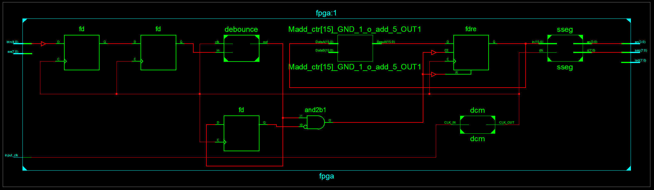
You can see that the “debounce” and “sseg” modules are represented as boxes here. You can double-click them to expand them in this schematic, but instead I’ll right-click the debounce module and select “New Schematic with Selected Objects”, and get this:
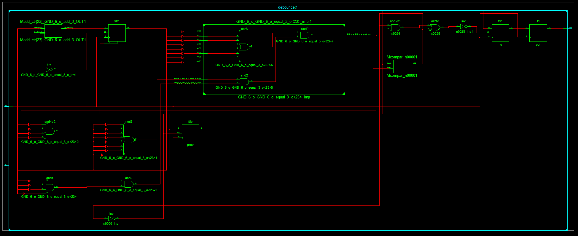
The prominent feature of this schematic is all the large-fan-in gates, that add up to a giant AND gate: this is the “ctr == N” piece of code. This makes sense: if we really want to verify that the counter is exactly 100,000, we’re going to have to check all bits of the counter. We can make the circuit considerably simpler by saying that the threshold must be a power of two; this means that we can change the code to just check a single bit of the counter, reducing the circuit to this:

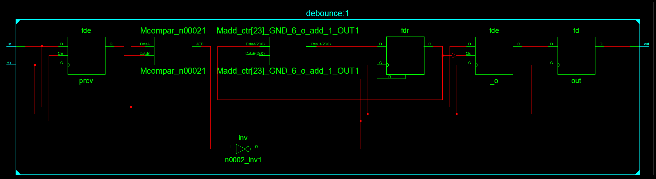
This looks much better, though there’s still some more that we can do. First, what’s this “Mcompar_n00001” node? This is saying that we shouldn’t update _o unless prev == in. This is pretty reasonable and seems like an optimization if you think of the updating as being costly, but in reality it’s the conditional that’s incurring expense here — this was a mindset shift for me, since in a programming world, “doing stuff” takes time, but in circuits everything is always active. I bet that this philosophy changes once you start considering power usage and the fact that “doing stuff” takes power, but if we’re just considering timing it’s actually more efficient to make the update happen all the time. So let’s change this to say that we’re willing to update _o even if prev != in — this only makes a difference if on the final cycle, where we’re about to update _o for the first time, we see that the input has changed, so essentially we’re changing the debouncer to only require N-1 constant inputs, instead of N.
Next, it’s a little hard to see from the schematic, but we’re using a “fdre” block for storing the counter: the “e” in the name refers to the fact that it has an “enable” input, which is currently being triggered off of the high bit of the counter — in other words, this register will stop being updated once the appropriate count is reached. The circuit could be simpler if we let the count always increase, but would what happen? It will eventually wrap around and retrigger setting the output again; but if this happens we’ll just harmlessly set the output to the same value, so the functionality will be the same. Once we make all these changes, we arrive at this much better-looking schematic:
Looking at the place-and-route report again, we see this:
Slice Logic Utilization:
  Number of Slice Registers:                    76 out of  18,224    1%
[snip]
  Number of Slice LUTs:                         84 out of   9,112    1%
[snip]

Slice Logic Distribution:
  Number of occupied Slices:                    29 out of   2,278    1%
[snip]
I’m actually surprised to see this, since I expected a larger improvement. When I did these debounce optimizations in an earlier version of this project, I ended up with a substantial area reduction, though as the whole first part of this post was about, it’s hard to reason about the exact output of the optimizers in an underconstrained project.
So, not sure if this was useful in the end, but you can see the final code here.
