A couple weeks ago I wrote about how I was building a brushless motor (BLDC) driver board, for the ultimate goal of using them in a quadcopter design. Well, the boards came in about a week ago and I’m finally ready to show off what they look like — and maybe complain about how much work they were in the process 😛
The boards
You can check out my previous post for more about the exact design (or find the source code on my github), but as a very brief summary, there are three main stages to my board: the digital/control stage, the power stage, and the back-emf sensing stage. The digital stage is mostly centered around an ATmega328 which controls the pwm, commutation, and does the back-emf sensing; the power stage involves six high-efficiency mosfets and associated components, and the back-emf sensing stage is an LM339 comparator and an analog mux that feeds it. Here’s the board design I came up with:

And here’s what these things looked like when I got them back from OSH Park:

These are by far the most involved boards I’ve made so far, and I still definitely get a rush seeing my design turned into a fine-precision physical object. I bought six boards, even though I only need 4, originally because OSH Park sells boards in quantities of three, but it turned out to be quite nice to have extras. I bought enough parts to assemble just one of the boards, since my I didn’t have too much confidence in the boards or part selection, and then set off to get the first board working.
Assembly woes
I started hand-soldering the first board, and things were going ok for a while: I feel like I’m starting to get the hang of TSSOP/QFP/0402 parts. There are definitely things about the layout that made it tough to assemble, that I want to avoid in the future: I put some components too close together, making it tricky to keep their solder separate, and some components were very difficult to place and access once the surrounding components were in place (in particular, the 0402 decoupling caps between some of the ICs). But these issues were dwarfed by the trouble I had with another problem: bad footprints.
I’ve been getting most of my package footprints from the SparkFun eagle libraries, or directly copying the manufacturers recommended land pattern when I need to create a new part. I guess I got a little overconfident with this board, because I used a couple new SparkFun footprints without verifying them first, which ended up causing a depressing amount of desoldering+resoldering+touchup work on those parts. First off, I’m not really sure how this happened, but their 0805 footprint is way smaller than I expected compared to an 0805 part; the pads are only as wide as the component itself, which means that you need to leave extra space around the pads for the component itself (as opposed to their other footprints such as 0402/0603/1206). Luckily I only had one place where this was really an issue, with three 0805 parts next to each other; for the subsequent boards I side-stepped this issue by putting 0603 caps on those footprints, which turned out to be fine.
The big problem, though, was with the resistor array footprint I used. This was my first board where I used these parts; they seemed pretty promising, giving a pretty good area reduction and reducing the number of components (if not the number of pads). I grabbed the RES-ARRAY footprint from the SparkFun libraries, and put 8 of them on my board. Big mistake.
The SparkFun footprint was totally different than the parts I had ordered. I’m not really sure how this happened, but the pads ended up being too close together, and also too short, which meant that the component completely covered the pads when placed. This meant that it was extremely hard to get solder to the pad, especially when hand-soldering, but I also had difficulty reflowing these parts (though that did turn out better). I went through many many many many cycles of desoldering the array, desoldering the pads, resoldering the chip, removing extra solder, checking for opens or shorts, and repeating. I definitely spent the vast majority of my touchup/debugging time on these parts… and unfortunately I have more boards coming in with the same footprint. Luckily, even though the footprint wasn’t that close, I was able to eventually solder all the resistor arrays, and I didn’t have to scrap the boards.
The last part of the assembly was the power stage, which posed it’s own challenge: I designed the power stage to handle high current (I was shooting for 20A though I doubt it can actually support that), which means that there are large copper pours with lots of thermal conductivity to the power stage components. At one point, I actually got the soldering iron stuck to a blob of solder — it was wicking away so much heat that the solder was able to solidify onto the iron! It was also interesting to solder the exposed pads of the mosfets: I put a number of vias on the pad for this purpose, which actually worked quite well (maybe too well, since I ended up using too much solder).
After many hours of work, I finally got the board assembled:

Getting it to work
I’m going to skip past the part where I spent hours tracking down an issue I thought was with the design but turned out to be just another short in one of the resistor arrays. After fixing all of those, I got the digital stage working, and the power stage working as well. I complained in the past about how difficult it is to debug a sensorless bldc design, because the back-emf sensing only works at high speeds. On the other hand, it definitely was nice that the three stages (digital, power, back-emf sensing) could be addressed sequentially: I first left the high-voltage disconnected, and tried to see if I could get the ATmega to work; then I connected the 12V rail and tried to see if I could slowly step the motor without any issues.
I had a lot of problems when it came to the back-emf sensing stage, though. I overbuilt this part of the system to give myself flexibility if I wanted something different: I feed the three sense inputs through an analog mux, since you only need to ever look at one of them at a time, and then fed the selected voltage into a comparator, where I compared it against three reference voltages, and then fed the outputs into the ATmega. I breadboarded something similar, but I hadn’t used an analog mux or this particular comparator, so suffice it to say, my design didn’t work out of the box.
The first issue is that I bought the wrong part. I don’t know how this happened… but I designed for a 4052 dual 4-to-1 mux/demux, but instead I bought the 4051 8-to-1 mux/demux. No problem, I’ll just put the 4051 on a breakout board and manually wire it up:

No luck — it’s still not working. Using my DIY scope, the issue seems to be that the analog mux was clipping the output voltage at 5V — which is weird, since the datasheet says you can control large voltages with logic-level inputs. Reading it again, though, it specifically meant large peak-to-peak voltages, which is assuming that your negative peak goes far below ground, to the analog negative rail. I have no idea why this part includes two negative supplies instead of two positive supplies, but the result is that I actually needed to power this chip from the 12V rail, but when doing this, it no longer takes logic-level inputs (Vih=10V)! So even if I rewired the board to supply 12V instead of 5V, I’d still need to shift up the control inputs, which involves a few more components than I think can really be bolted on. Things were looking kind of bleak.
Then, I decided to try something: I hard-wired just one of the sense inputs to the mux, and changed the software to only do back-emf sensing one third of the time, when that specific phase was idle. It turns out that this ended up being fine! I suppose that I could have better or faster control of the speed by sensing it three times as often, but qualitatively the motor seems to drive just fine.
I wish I had taken a picture or video of it at this point, but to my huge relief the board was successfully driving my test motor. So, it was time to order more components for the other boards.
I decided to slightly change the components to reduce cost; I decided to make four additional boards (I didn’t trust my prototype board after cutting it up so much), and that plus the RC supplies were starting to add up in cost. I made two substitutions: I used cheaper 4mΩ MOSFETs (the original ones I picked were 2mΩ), and I switched from ATmega328’s to ATmega88’s, since the code size was relatively small. Also, I ordered a stencil for the board, partially because I wanted to try stenciling and I found OSH Stencils (no relation to OSH Park) that produces them pretty cheaply.
Fast forward to getting the new parts…
Assembling the other boards
My plan was to first assemble board #2 (the original hand-soldered board was board #1), to make sure the new stencil+reflow process worked, and then assemble boards #3 #4 and #5 at the same time. Here’s my first-ever attempt at using a solder paste stencil:

I tried to not put much on there since I put those vias on the MOSFET pads specifically for hand-soldering, but I was worried that in reflow the solder would get sucked through (which it did). Even ignoring that, the paste application was pretty bad; I must have jostled the stencil or board while I was applying it. (Pro tip: apply the paste away from the fingers you’re using to hold the stencil, to best keep the stencil flat and in place.) Here’s a closeup:

My past experiments with reflow soldering showed me that it’s far more important to have the right amount of solder, and the process is hugely forgiving to the exact placement of the solder. So, despite the fact that most of the footprints have barely-discernible smears of paste, I decided to go ahead with this board. Either way, it will give me good insight into how precise the solder application needs to be.
Well, the answer is a little more precise than what I did, but not too much more:

Above is the result: everything is in the right place, but you can see several solder jumpers in the above picture, along with a decoupling cap that has been completely claimed by one of its pads and is sitting vertically. All in all, I was actually pretty impressed by how the results came out — this is far fewer jumpers than I would have created soldering this by hand. I just went through with some desoldering braid and cleaned it up, and used the multimeter to show that electrically things looked good. Except, of course, for the resistor arrays… I had to pull a bunch of those up and resolder them by hand. In fact for this particular board I was unable to get one of the arrays soldered before ripping up its pads; luckily it seems like those resistors were superfluous anyway, so I just replaced them with 30AWG wire.
Migrating from an ATmega328 to an ATmega88
So, according to what I read on the interwebs, the ATmega88 and ATmega328 are supposed to be interchangeable. What I found was that while, yes, they are pin-compatible and use the same instruction set, you can’t just drop one in for the other and expect it to work. There are a few reasons why, apart from the obvious one that they have different amounts of program flash and RAM:
- The interrupt tables are different. In the 88, each interrupt vector is 1 word (2 bytes), but in the 168/328, they’re 2 words (4 bytes). This isn’t too big a deal, since the compiler will generate the right table for you (or maybe it’s one of my libraries, not sure), though you do have to tell the compiler that you’re targeting a different part.
- The fuses are very slightly different; this was probably more confusing than actually damaging.
- Finally, the generated code is different, with slightly different timing characteristics! I’m not 100% sure what the exact cause is, but my guess is that it’s because the compiler emits “rjmp” and “rcall” instructions on the 88 instead of “jmp” and “call” on the 328. Tiny differences like this probably don’t matter for most projects, but I’m trying to commutate the motor with sub-microsecond accuracy, and the reduction in function call time drastically changed the timing parameters required.
In the end I got the ATmega88’s working just as well as the 328’s, and learned more about them in the process, but I’m not sure if I’ll do this again. This is especially true due to the fact that the price savings from going from an ATmega328 ($2.77) to an 88 ($2.13) is less than from buying the 328’s in bulk ($1.74 @25), so for ATmega’s it seems more worth standardizing a part and buying more of them, than trying to pick the perfect part for each project. I didn’t want to do that for this project, since I’m not sure if I’m going to stick with TQFP parts or if I can make the jump to QFN parts — but that’s a different story.
There was one last problem with the board: I had removed the 4052 part from the design, but that unfortunately didn’t mean I could ignore it, since its footprint and traces were still there. If you look at the top part of the above photo, you’ll see that there are a couple jumpers on the unpopulated footprint; the one on the right is a jumper between the 5V rail and a motor lead, which needless to say, caused havoc until I cleaned it up.
Building the rest
Now, it’s time to build the other three boards. At this point, after several nights of working on it, I’m getting pretty tired of soldering, especially for these boards. My hope was that by assembling all three at the same time, I could significantly cut down on the assembly time. For instance, I find that when assembling a board I seem to spend more time “picking” than “placing” components, at least with this design where there are many different components (many different-value resistors, for instance), and my hope was that by doing three boards I could amortize the picking across three times as many placings.

It turns out that I was mostly right: while board #2 (the first reflow board) took me about an hour to solder, boards #3 through #5 took a combined 90 minutes to solder. It’s not really a fair comparison since there was some aspect of me overall being faster at these boards (the time-per-board would have gone down even without doing multiple boards at once), but it was definitely a welcome speedup. The big difference, though, was in the touchup and debugging stages. First off, my solder paste application was better, requiring fewer manual adjustments — but still some, so I still need to work on my process:
The big wins, though, came from reductions in the debugging time. At this point I only ran into issues that I had already had with the first two boards, and I had already mapped out the hot-fixes I needed to make, so I was able to make all three boards in a night, as opposed to the first two boards which each took an entire night themselves.
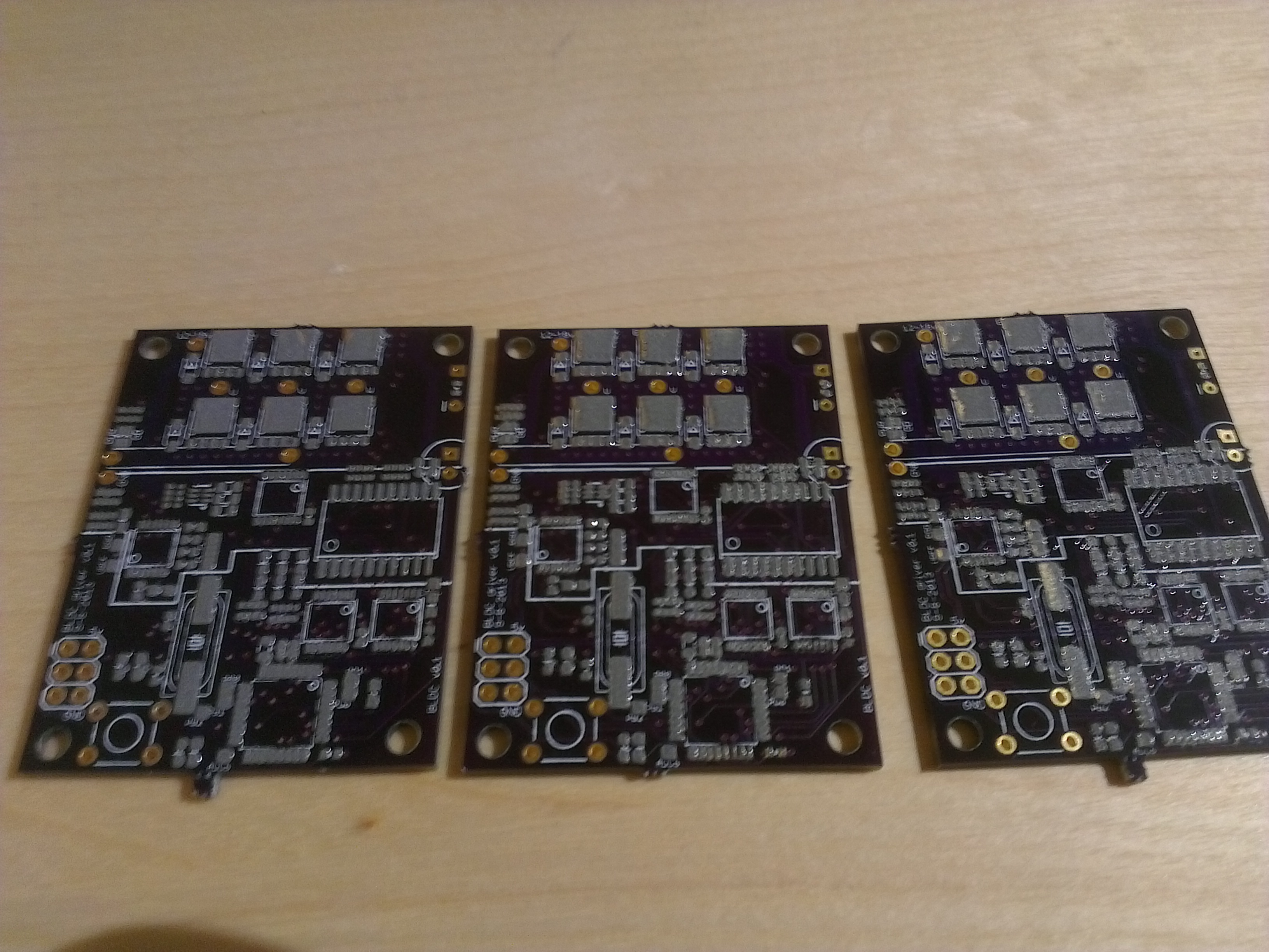
Final product
I haven’t taken any videos yet, since right now I can still only run one motor at a time (due to power supply limitations), but here are my assembled boards:

I assembled them left-to-right, top-to-bottom (board #4 is in the bottom left), and you can see the marked reduction in extra wiring.
There are a lot of things I would change if I wanted to put together a v0.2. For instance, I didn’t put a pull-down resistor on the PWM line, which means that when I hit reset the driver input will be left floating, ie the mosfets will still be on! I found this important enough to change that I actually soldered 10k resistors onto these boards. There are also a number of places where I deliberately overbuilt the circuit to leave headroom (there are still features I want to add) and in general I think the 20A target was way too high — running a single motor at 1A is enough power to blow things off my desk, and forceful enough that I feel the need to wear safety glasses while testing. If I were to start from scratch, there are also some all-in-one BLDC driver chips that could have replaced… pretty much all of my circuit.
But the boards are working, so that’s it for this step! I’m not sure how much current these things can handle, but at 1A the boards didn’t even feel warm at all, and based on feel, I think 1A is more than enough current to hover the copter, so I may never fully stress these things. From here, I need to attach the final wiring solution (18AWG wire instead of 22, and with proper connectors on the end), and follow through with my plans to create an ATX-to-XT60 connector that would allow me to power all four boards from an old computer power supply, at which point I should be able to drive all four motors at the same time, and hopefully achieve (uncontrolled) flight! The final piece of the copter is the central control board, which I just got a notification that OSH Park has shipped and should be here in time for the weekend 🙂
