So I decided to try my hand at BGA reflow; this is something I’ve wanted to do for awhile, and recently I read about some people having success with it so I decided to give it a shot. I’m trying to start moving up the high-speed ladder to things like larger FPGAs, DRAM, or flash chips, which are largely coming in BGA parts (especially FPGAs: except for the smallest ones, they *only* come in BGA packages). I’ve generally been happy with the reflow results I’ve been getting so I felt confident and tried some BGAs. It didn’t work out very well.
First of all, the test:

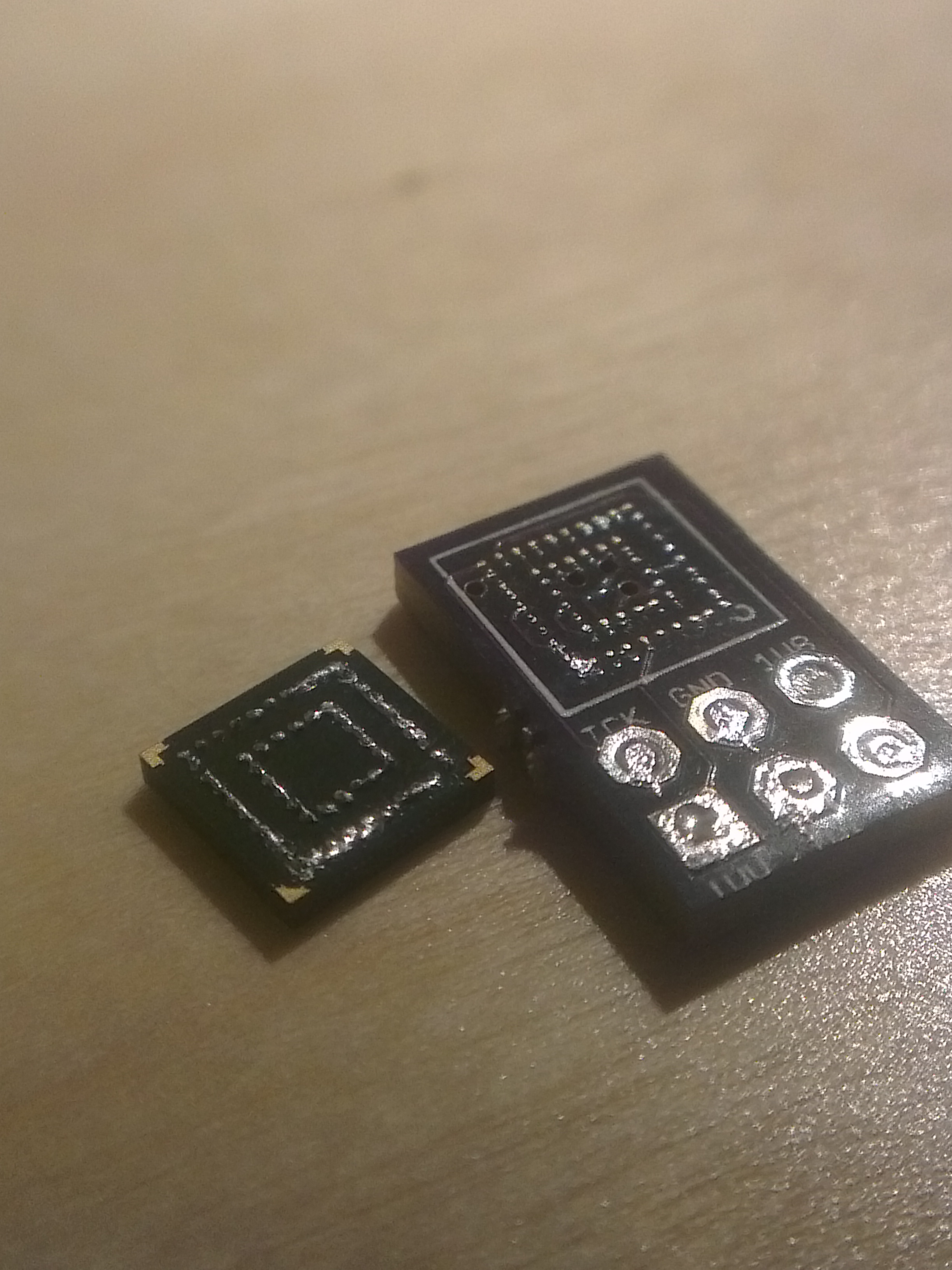
This is a simple Xilinx CPLD on the left, along with a simple board that just has the BGA footprint along with a JTAG header. The CPLD costs $1.60 on Digikey, and the boards were incredibly cheap due to their small size, so the entire setup is cheap enough to be disposable (good thing). This CPLD uses 0.5-mm pitch balls, which is really really small; it’s so small that I can only route it because they only use two of the rows. It also means that getting this to work properly is probably in some ways much more difficult than a larger-pitch BGA, which is good since in the future when I use those, they’ll have many more balls that need to be soldered reliably.
Test 1
The first test I did was, in hindsight, probably the one that worked out the best. What I did was applied some flux to the board using a flux pen, carefully placed the BGA, and reflowed it. An unexpected complication to this process was that since the only thing being reflowed was a BGA, I had no visual indication of how the reflow was going! This is important to me because I don’t have a reflow controller for my toaster oven, so I just control it manually (which works better than you might think). I did my best to guess how it was going, and at the end the chip was pretty well-attached to the board, but I felt pretty in inconfident in it.
I hooked up my JTAG programmer, and had it spew out a stream of commands that should get echoed back: what I got back was a constant 1.8V signal (ie Vcc). I was disappointed with this result, since I really had no idea how to test this board. In retrospect, that constant signal was quite a bit better than I thought: it means that at least three of the pins (1.V, TDO, and presumably GND) were connected.
I was still feeling pretty bad about the soldering reflow, so I decided to try putting it back in the oven for a second go. Turns out that that’s a pretty bad idea:
So I moved on to test #2
Test 2
I used the same exact process for the second test as I did for the first, though this time I put some “indicator solder” on a separate board just to get a visual gauge for the temperature. This test ended up being pretty quick, though, since I was too hasty in aligning the BGA (or maybe I knocked it out of place when transferring it to the oven), and it came out clearly-misaligned. I put it through the tester anyway, for good measure, but then moved on to the next test.
Test 3
For the third test, I used tacky gel flux, instead of liquid flux from a flux pen, to see if that would help. Unfortunately, I think the problem was that I added way too much flux, and there was so much residue that the solder balls did not make good contact with their pads. In fact, as I was soldering on the test pins, the CPLD came off entirely.
At this point, I was out of CPLDs to test on — you only get one shot at reflowing them, unless you’re willing to re-ball them (which is probably much more expensive than just buying new ones anyway). I ordered a bunch more, so I’ll take another crack at it soon. The things I’m going to try are:
- Using liquid flux again but with a solder indicator and not messing up the alignment
- Using gel flux again but with less of it
- Using a stencil with solder paste, instead of just flux

3 responses to “First trials with BGA parts”
Thanks for the inspiration! I set out to duplicate your board so I could test my own BGA reflow process, but when I realized that I could (barely!) escape all the pins with the 4-layer OSH Park design rules, I couldn’t resist!
https://oshpark.com/shared_projects/7wvUxq8S
Rev 2 could use some thermal relief on the 0.1″ header through holes and the capacitor pads for easier hand-soldering.
LikeLike
Success! http://imgur.com/zWavHQj
My first try was with a kapton stencil from oshstencils and leaded solder paste. the result looks OK mechanically, but I couldn’t get the board to JTAG. leaded solder paste with lead-free solder balls on the package doesn’t work too well. the second try (pictured) is with no-clean paste flux brushed on the part and the board, no solder paste, and it worked like a champ.
once I get some lead-free solder paste, i’ll try the stencil again. initially i had some concerns about being able to reliably deposit solder paste by hands on pads that small (without sticking to the stencil or smudging), but after following the stencil aperture calculations outlined here ( http://www.ti.com/lit/an/swpa156/swpa156.pdf ), that part of it actually worked great the first time.
LikeLike
Congrats!
That’s a really good point about mixing leaded/lead-free solder, and might explain some of the issues I’ve been having with DDR3 packages.
LikeLike