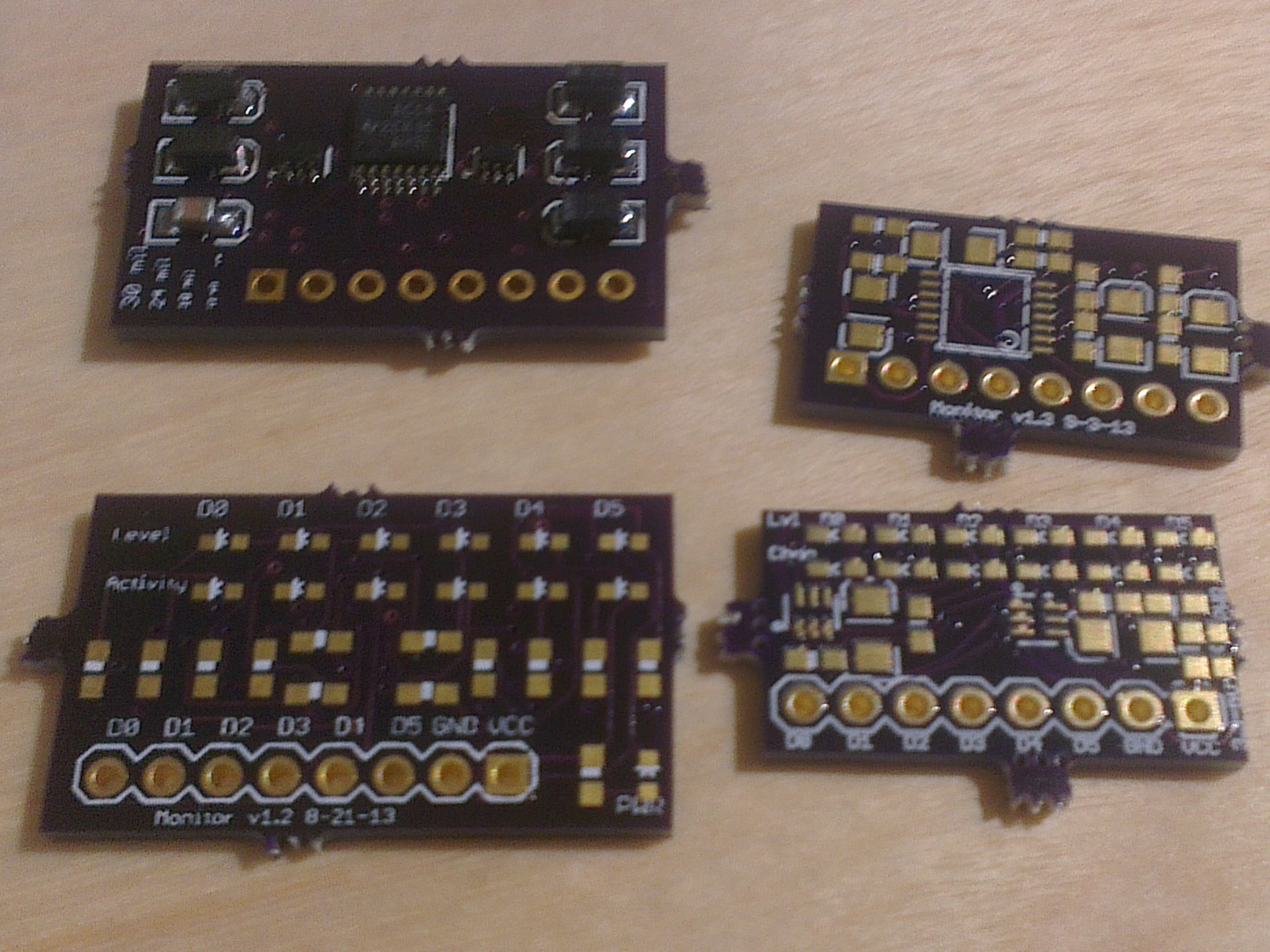
I’ve done a series of circuit board layouts of my simple “Activity Monitor” circuit, at first to teach myself PCB design and try out getting them made, and lately to test different different pcb limits, primarily miniaturization. In my last post about it, I talked about putting together a board I thought was high-density, and how I submitted a new design that was even more dense. Well, I got back the boards today and here’s how it went. First up, here’s a picture comparing the four iterations of the boards:

The left-most board is my first attempt, and the first circuit board I ever created. It uses through-hole components exclusively, and measured 1.69″ x 2.55″. The green boards are my second attempt, my second circuit boards ever, and my first experimentation with surface-mount components. I could have made this smaller if I wanted but the goal for that iteration was to try out SeeedStudio (hence the non-purple color), and to test smd components.
The next pair are my first attempt at miniaturizing the circuit, using all surface-mount components and taking out “extras” like the mounting holes and second (duplicate) pin header. I also bumped up the number of signals from 4 to 6, so there’s actually about 50% more logic in this board than the first two iterations. Since this was such a reduction from the previous iteration, I didn’t want to shrink it any more than this, despite thinking that I could. Here’s a close up of the most recent iterations:
As you can see, I made the fourth and final rev smaller mostly by taking out the spaces between the components, but also by breaking symmetry and hand-routing the board, allowing me to pack the components this tightly, getting down to a final size of 0.85″ x 0.48″. Here are pics of the soldered board:

Sorry for the poor image quality — I had to take these through my cheap 10x loupe to get any reasonable level of detail.

There are a few things I learned from this: the first is that average density doesn’t matter at all; all that matters is local density (ie space on the other side of the board doesn’t make the current side any easier to solder). When I was making these I was worried about “how small the board is compared to the number of components”, but this really doesn’t matter compared to how close any two individual components are.
The second thing I learned is that the order in which I soldered the components is even more important at this scale. The method I’ve settled on for most boards is 1) tin one pad for each component 2) pick out all the components for a type and attach them to their pads 3) go back and fully solder all the components. This didn’t work out so well on this board, since by the time I had placed the 1206 capacitors, the TSSOP parts were very hard to get to. Instead, I fully-soldered the TSSOPs first, which made it much more feasible, though it through off my method.
This worked fine for assembly, but not for any rework: I wanted to change some resistors out (the new LEDs I tried were too dim), and I resorted to pulling off multiple parts in order to get access to the resistors I wanted to remove (if I had solder tweezers maybe this wouldn’t have been an issue).
The last thing is that I was somewhat validated in worrying about putting the pads close together: when I tinned a specific pad, the solder ran into the next one. It turns out that these were connected by a trace so it was fine, and perhaps the trace is what allowed the solder to run, but overall I am now more worried about that.
So in conclusion, I feel confident that this density is hand-solderable, especially now that I have 0.012″ solder and a 0.4mm soldering iron tip, but I’ll probably scale back somewhat, especially around “tall” items like the 1206 capacitors (which I’m not planning on using anymore anyway).

One response to “PCB miniaturization: the limit”
Hi,
I was looking for some information on PCB Assembly today when I came across your awesome website.
Great stuff!
Actually, I just put together an infographic about “Assembly Methods for Printed Circuit Boards”. As someone that who’s on Electronics, I thought you might get a kick out of it.
Let me know if you want to check it out.
Cheers,
Algen
LikeLike