I’ve recently been intrigued by the idea of using CPLDs in my designs — there have been lots (maybe 2 or 3!) of times that I’ve wanted a specific set of glue logic, only to find out it doesn’t exist or the output polarity is wrong, and I have to resort to using multiple 74xx chips. A CPLD seems like a natural solution to this: as mini-FPGAs (perhaps more correctly, FPGAs are mega-CPLDs), you can configure them to perform a large range of combinatorial logic, and you can get exactly the “part” you want. This means both the exact logic behavior, but also the more-or-less exact pin placement, which I’m increasingly discovering the importance of. CPLDs are pretty cheap, starting at about $1 on the low end, which is the price of two 74xx chips. Clearly, they’re going to be more complicated than just snapping some off-the-shelf parts in, but it seems like they should be a relative shoe-in.
This is the story of me getting started with the Xilinx CoolRunner-II cplds.
SMD-only
The first issue is that CPLDs, at least CoolRunner-IIs, only come in SMD packages. Thankfully the situation isn’t as bad as FPGAs, where almost all parts come in BGA packages, but it means that I needed to find a TQFP adapter for prototyping (part of the reason why I wanted to make my own). Here’s a picture of the 0.8mm-pitch chip soldered onto the adapter; I was worried about the extra-long adapter pads making this hard to solder, but it turned out to be fine:

Here’s the rest of the circuit this is a part of:
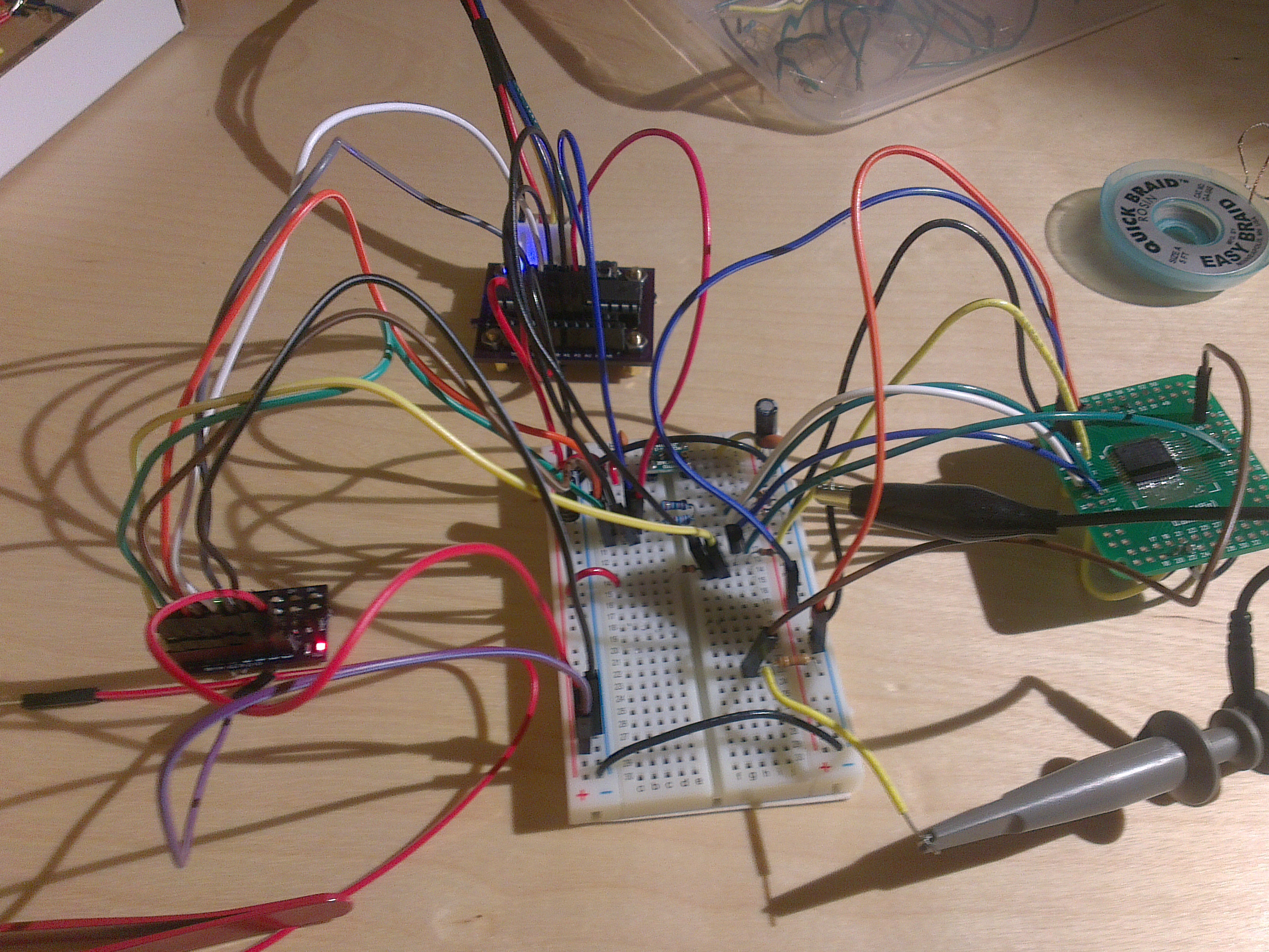
There’s not much on the breadboard in the middle, just a 1.8V voltage regulator, and some level-shifting circuitry (more on that in a sec). On the left is one of my “activity monitors” that was actually useful for debugging (good thing I’ve made 20+ of them for testing purposes!). On the top is a little ATmega328 board serving as a JTAG programmer.
Voltage levels
The first hiccup I encountered was with voltage levels. The CoolRunner-II has four supply voltages: a 1.8V “core” voltage, and three adjustable voltages (two for the two IO banks, and one “auxiliary” for the JTAG interface). I was prepared for the idea of the cpld requiring a lower voltage, even though it would mean adding a 1.8V and 3.3V supply.
Once I started to look into it further, however, I uncovered more issues. First of all the CoolRunner-II is *not* 5V tolerant, even with current-limiting resistors (ie there’s a voltage limit separate from a current limit). Unlike most parts I’ve dealt with (such as the ATmega328), the CoolRunner-II doesn’t have ESD protection diodes, which automatically clamp the input voltages into typically-acceptable ranges. Although you have to worry about the current you send across those diodes, this means you can interface a higher-voltage signal to a lower-voltage part simply by putting a current-limiting resistor in series. Unfortunately, this doesn’t work for the CoolRunner-II, which means that you have to use some other method, typically involving at least two discrete parts, or a fraction of a different IC that can do this level-shifting. For most uses this isn’t that bad, but for the purpose of reducing the “glue” complexity in the system, it’s a step in the wrong direction.
Let’s ignore this for now; my thoughts are that I’ll probably move designs involving cplds to using a main supply voltage of 3.3V. As a sidenote, technically running an ATmega at 16MHz and 3.3V is out of spec (ie overclocking), though reading on the internet this seems to be a common thing that people don’t report issues with (the issues probably happen at one of the temperature extremes). For the testing, I wired up some resistor divider down-shifters and a simple NPN up-shifter, since I was running all four voltages at 1.8V.
JTAG
Now that I had the chip powered up, the next step was to get it to do something. The CoolRunner-II, and most of Xilinx’s (and I presume other peoples’) parts are programmed over a 4-wire interface called JTAG. I won’t really get into the details of JTAG, but for a single chip it looks pretty much like SPI, but the benefit is that it’s designed for hooking multiple chips into a chain, so that you only need 4 wires regardless of the number of chips you have (in theory).
When I encounter a new protocol, I usually put a simple shim program on my ATmega328, which listens on the serial interface and allows a computer script to control all the IO pins. This means I can use Python on my computer, avoiding recompiling+reprogramming, plus giving me more control and visibility into the program. The downside, of course, is the overhead, but for trying out new protocols that’s not as important. You can find the code here, but in essence it allows you to write the “Blink” Arduino sketch like this:
controller = DebugController("/dev/ttyUSB0", br=500000)
controller.pinMode(13, "output")
while True:
    controller.digitalWrite(13, 1)
    time.sleep(0.5)
    controller.digitalWrite(13, 0)
    time.sleep(0.5)
Using this, I wrote a very simple Python script that let bit-bang’ed the JTAG protocol and was able to get the chip to respond! It took me a few tries to get the bit timings exactly right (ie when exactly a bit is read by the cpld, and which clock cycles the cpld’s outputs correspond to), but I was able to eventually read the part IDCODE out.
The next step was to actually get this thing programmed. I won’t go into how to write the program for it, but suffice it to say that Xilinx’s tools are able to produce a “SVF” file, which is essentially a list of JTAG operations that will result in the chip being programmed. Luckily, SVF is a very simple format and the main hard part in writing a SVF reader+player is to understand JTAG.
I only implemented the subset of SVF that the Xilinx tools output, so it was surprisingly manageable to write the player, which you can find here. I excitedly started running it on the full programming file, and… it took 5 minutes to program the CPLD. The obvious thing to do would be to port the SVF player to the ATmega328 and just send the SVF file down instead of the bit-bang instructions, but I didn’t feel like doing that; after some performance debugging, I found the issue was that I was waiting for the ATmega328 to respond to each command before issuing the next one, so I changed it to only block when the SVF specified to verify the output, which tends to be at end of long transfers. I was able to get the programming time down to 25 seconds, which is starting to be bearable, but if I do end up using CPLDs I hope I have time to rewrite the programmer.
Anyway, at this point I had a CPLD programmed as a single XOR gate, and it was something of a rush to see it finally respond when I changed the inputs 🙂
Improving the build process
One thing I’ve always been slightly annoyed with when it comes to Xilinx development is how tedious it can be to do a compile-and-reprogram cycle. For FPGAs, it involves double-clicking a small list item in the ISE interface, waiting, then going to the Impact program, and clicking another rather small button. This is worse with new custom programming step, since I have to use Impact to generate the SVF file, then go to the shell and program the device.
I thought about adding support for my programmer in Impact, or creating some sort of custom script in ISE (which I’m vaguely aware is possible), but this quickly turned into a dead end. Instead, it was much simpler to simply take the commands that ISE itself runs (with some help from this site), and put them into a Makefile so that I can live on the command line. Again, it took a couple tries to get right — if you don’t erase the CPLD first (the default is to not erase) it won’t program correctly — but eventually I had a working Makefile that could all-in-one program my cpld with only one command and no mouse clicks. You can find the example project here.
Breakout board
Now that I was confident in being able to use the CPLDs, the next thing I wanted to do was create a simple breakout board with some switches and lights. Here’s what I came up with:

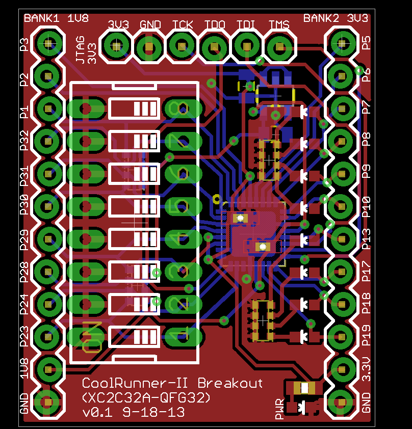
It’s definitely not as full-featured as a real CPLD breakout board, but I just wanted to throw something together quickly for testing. It takes a 3.3V supply voltage, and has an on-board 1.8V regulator. It runs the two IO banks at different voltages, one at 1.8V and one at 3.3V. There are eight slide switches and eight leds, which should hopefully be better for debugging than moving wires around and looking at the multimeter.
Update: I just noticed that I have the two IO banks backwards. This mainly means that the voltages on the two banks are swapped, which means the LEDs won’t work without some hot-fixing.
Other ideas
One thing I want to do with this is create a simple ATmega project board, but with a CPLD as configurable router. Most of my projects only involve a few IO pins on the ATmega, but those pins tend to differ project-by-project. I tried to think of ways to reduce the pin count on the board, such as by connecting multiple pins to the same pin header, but using a CPLD seems like a way around this.
Also, since CPLDs are somewhat like miniature FPGAs, I think I’m ready to put together my first FPGA board. But first, my BLDC driver boards have arrived, so I’ll probably play around with one of those.
