I spent all yesterday dealing with some mistakes I had made in some boards; I thought I’d blog about it because 1) I spent time on it and want to feel like something came out of it :P, and 2) because I think it might be interesting to someone. Personally I find it very interesting to read about things that go wrong, since I think that that can give a better idea of how to accomplish something than just seeing a success story. When I first started out making circuit boards I had a vague idea of what kinds of things are important, but had no idea what that meant I should actually worry about, so as a result I ended up worrying about everything! Now, I’m starting to develop a sense of what types of things I tend to regret about my designs and I’m gradually getting more focused, but I definitely have a ways to go.
This post is about two specific circuit boards that I made multiple mistakes on, but I thought it’d be worth mentioning what things I normally don’t like about my boards. The most common thing I run into is not knowing how to “design for manufacturability” (DFM); on every single board I find myself thinking that the board is obnoxiously hard to validate once it’s assembled. Typically this means that I don’t have test pads or labels for signals that end up being important; I’ve learned to always break out and label power nets, but I still find myself trying to touch my scope to the specific pin of a TSSOP part (the hardest part is looking at the screen while not shorting that pin to an adjacent one!). This is pretty clearly a balancing act; I could break out every single signal, or go back to through-hole parts, but at a cost to circuit bulkiness. One thing that I’ve found quite helpful is to expand the pads for almost all of the footprints I use, since the extra board space is negligible (it would usually be part of a route-out), and it helps a lot with hand-soldering or hand-testing. Anyway, these kinds of DFM things are probably what I think about the most now during the layout part of the design.
The second thing I end up running into is that after I have the board built, I wish that it worked differently or had additional features. Sometimes this can be addressed by leaving do-not-populate parts on the board, though at my typical quantity of 1 assembled board per design, I tend to just cut traces and green-wire when necessary. The second part — wanting the design to have more features or be different in some other way — I view as a natural part of any engineering process so I don’t feel too bad when it comes up, but trying to make the board “feature-complete” is what I think about the most during the schematic part of the design.
Maybe interesting to know is what I don’t worry about that much: I’ve never put too much thought into the routing of signals or power/ground nets (other than wanting to do it easily). As I’ve learned more about “grounding best practices”, I’ve realized how far I am from them in all my board designs, but it hasn’t seemed to affected any of them so far. This is probably due to the fairly small+simplistic designs plus the low max speeds (16MHz), but so far I’ve been able to avoid worrying about those kinds of things. That said, having good grounding (right now in the form of having *sufficient* grounding) is starting come up, and I suspect that these types of things will only be more important as I work my way into faster circuits.
Anyway, this was supposed to be a post about some mistakes I made; I don’t consider the things I just mentioned to be “mistakes” since they’re just things that I’ll have to continually improve on. I’ve started to rush my board-design process, to both decrease the time I spend on it but also force myself to make some mistakes to see what they are, and here’s what’s come up:
Barely-salvaged: power distribution board
I’ll talk about the setup more later, but I’ve changed my designs so that instead of each board having its own power input and regulation, I have some dedicated power distribution boards so that I only have to design + build that circuitry once. All good in theory, but this board has the privilege of being the first of mine to catch fire:
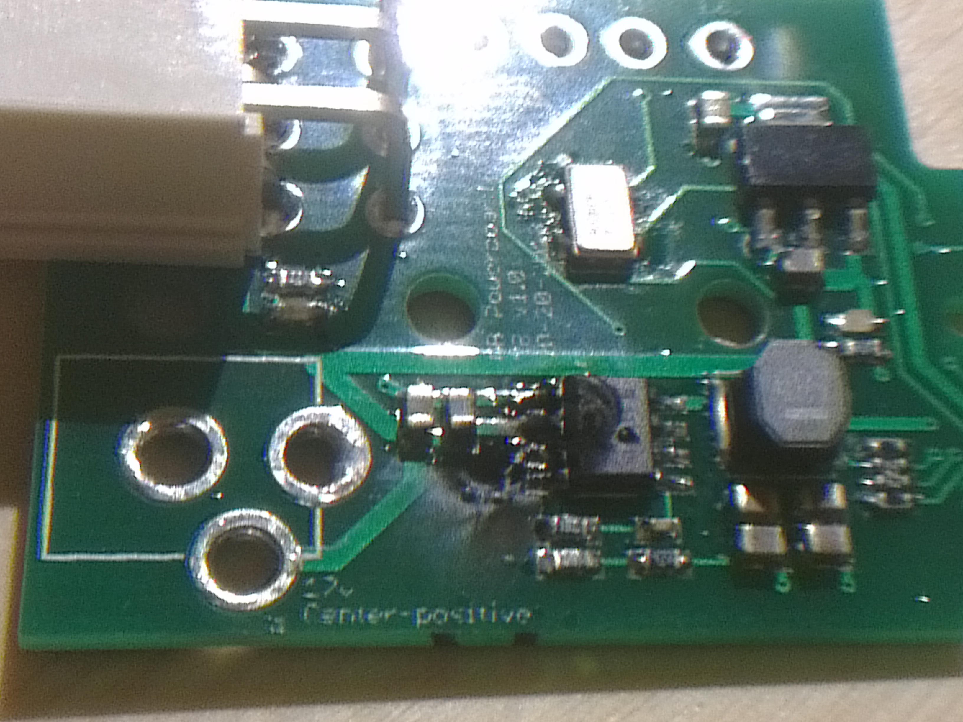
The fire wasn’t really a mistake in the circuit board design, but more in my usage of the board. That large beige connector in the top-left is a 6-pin molex connector, of the kind that you might find inside your computer. I put this on there because I have an extra ATX power supply lying around and I thought this would be an easy way to get lots of DC power. So after I assembled the board, I plugged in the power supply and POOF a fire! I’ve had chips smoke in the past, but this was a legit orange flame with hissing and crackling. My dog, who usually sleeps under my workbench, immediately ran out of the room. I cut the power and things were fine, though there was some obvious damage to the board.
What happened? It turns out that there are two different 6-pin connectors on this (all?) power supplies, one for the motherboard and the rest for PCI-express boards. Well, I had just grabbed the first one I saw and plugged it into the board: it turns out that the CPU and PCI-express plugs are keyed compatibly, but have opposite polarity! So instead of feeding my 12V->3.3V regulator 12V, I was feeding it -12V, and that was the end of that. This might have been avoided if I had put a reverse-polarity-protection diode; the power supply is perfectly willing to put out enough current to fry any reasonably-sized diode, so I would have needed some sort of over-current protection as well.
I was actually able to get some use out of this particular board; I had to remove the charred regulator, but then I just fed the board 3.3V directly and then the 1.8V regulator (upper right) worked just fine. But there are a couple more problems with the board that you might be able to notice.
The first is the unpopulated barrel-jack socket in the bottom left. You can see that the silkscreen calls for a center-positive plug, but the 12V line goes to what is definitely *not* the center of the plug. This was a result of me misinterpreting the schematic symbol for the Eagle part I obtained (from SparkFun, like usual), and not double-checking the board layout to make sure it matched my expectation. I wasn’t too bummed about it since this was just the backup way of getting power onto the board, with the ATX connector being the intended one. That being said, I think I would have rather had the barrel plug because that cable is much more flexible than the ATX power supply cable, which ends up more-or-less fixing the orientation of the board while I use it.
The second major problem with this board is the messed up oscillator, the silver box roughly in the middle of the board. For this one, this was a mistake in me reading the datasheet: for some reason I thought the Enable pin was active-low, when in fact it was active-high, so I in order to get it to work I had to cut some traces and green-wire.
I wasn’t able to get the 12V circuitry working on the board that had the fire — even after replacing the IC that caught on fire, the board didn’t work correctly. At that point I decided that debugging a previously-on-fire board was probably a losing battle, so I ordered the parts to make another one, which now works quite well (barring the missing barrel plug socket):

Not recoverable but still interesting: jtag board
I’m using JTAG a fair bit in my current project, for which I built my own JTAG adapter. It was an interesting exercise to understand how the whole thing works, but the result is pretty messy:

It’s a little tough to see from this picture, but the way this works is I have a USB connection from my laptop (grey cable coming in from the left), which connects to a CP2103 (USB<->UART chip) breakout board, which connects to an arduino-like board, which then connects to a breadboard where I’m doing level-shifting, which then connects down to the project itself (out of view). I’ve found the laptop->CP2103->atmega->breadboard toolchain to be quite good for prototyping and development, but it’s getting cumbersome and involves quite a few wires. So, I decided to coalesce all of this into a single circuit board in order to make it easier to manage, and here’s what I came up with:
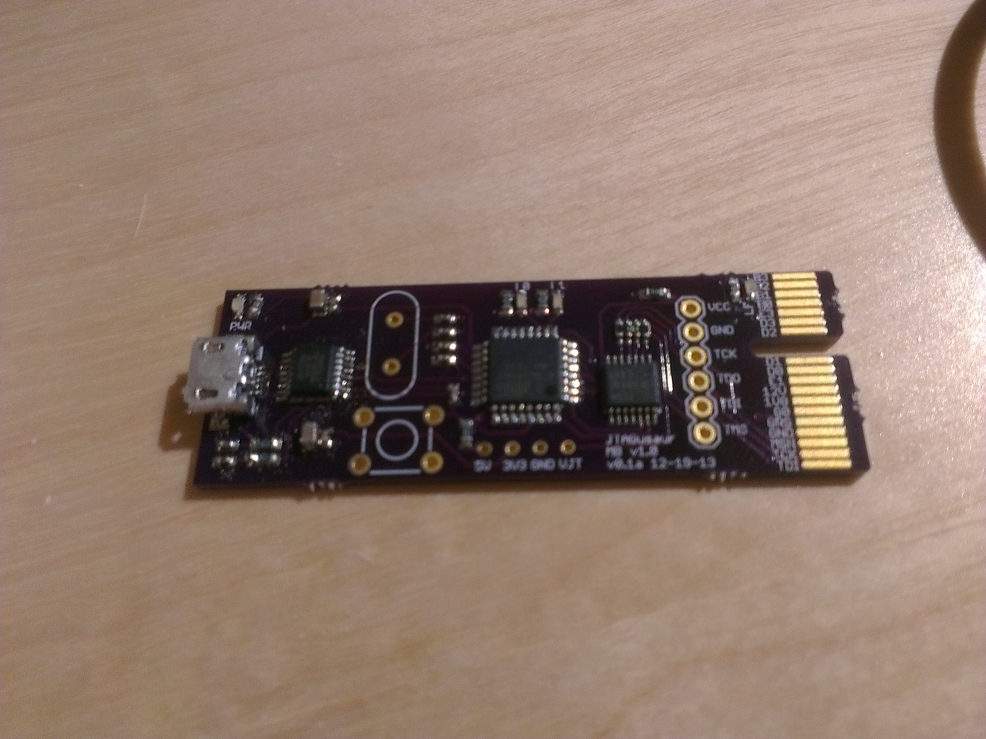
As you can see, the through-hole components are unpopulated because I realized that the board wasn’t going to work. This board has given me quite some trouble; here’s the first run of it, can you spot the difference?

The problem was that I used the wrong footprint for the FT230X, the IC right next to the USB port. (Note: SOP != SSOP, not by a long shot.) I noticed the problem pretty quickly, but only after I had sent out the design to OSH Park for boards and OSH Stencils for a stencil. It was a pretty easy fix, so within a day I sent the new boards to OSH Park, but I forgot to have another stencil made! So yeah, there were a few issues through that process.
I actually managed to use the wrong stencil for the board with reasonable results. The only main problem was that the USB connector was completely misaligned and not connected; not sure if this was a result of the wrong stencil or a bad footprint or what (I used a generic micro-USB footprint, not the one suggested for this particular part). Re-soldering the USB socket was particularly hard because the FT230X, the TSSOP next to the connector, is so close that it was very difficult to fit the soldering iron or multimeter probe in there. (This kind of proximity issue is actually one of my most common ones, and I’m still not great at anticipating it.)
So I got the USB port resoldered, but then I noticed two problems with the ATmega part of the schematic: first, I had forgotten an ISP header to flash the code. For my existing jtag setup I had pre-programmed the chip with a bootloader, and since it was talking serial I could use the bootloader to load new versions. My normal approach is to use my ZIF-socket-programmer to burn the bootloader for DIP chips, but this is a QFP so I was out of luck. What I did instead was I soldered it to another project that uses the same footprint and does have an ISP header, then burnt the bootloader onto it, then removed it and resoldered it to the current board. This was actually all-for-naught, since I burned the wrong bootloader code onto it, so I actually soldered tiny leads onto the four relevant IC pins, and then connected that to the programmer, and flashed the correct bootloader.
Actually, I wasn’t able to do that right away, since I noticed that I had messed up the ATmega crystal circuit. It’s a very simple circuit and I guess I assumed that I knew it well enough to not look it up again, and so of course it ended up messed up. I had to do some more greenwiring, which included soldering some through-hole capacitors onto the back of the board. But after I did this, I plugged in the USB and saw the bootloader flash the LED!
In the midst of all of this, the USB connector came off. This micro-USB socket has only SMD pads, and is very space efficient, but is very hard to hand-solder (I was doing this with the wrong stencil so I didn’t reflow this part). It actually left me in a pretty weird predicament since all the connections broke except for one, while the cable was still plugged in! Do I rip the last pad off, potentially lifting the pad? Do I use pliers to try to remove the socket from the cable without putting force on the board? (tried that and it didn’t work) Or do I use my soldering iron to undo that last joint? I was pretty wary of doing that last one, since I learned the hard way that for my fancy Metcal soldering iron the soldering head is actually electrically hot, and Bad Things can happen if I use it on a live circuit. After I tried using pliers unsuccessfully (not possible to get a good hold while the board was still half-attached), I finally just resorted to using it and everything was fine.
After reattaching the USB socket, I was able to boot up my circuit and use the bootloader to flash my JTAG programmer! Everything was going great until I then connected the adapter to my JTAG circuit, at which point it promptly stopped working — I don’t even get the led flashes from the bootloader any more. I’ll look into it more later, but for now I’m going to put my effort into designing v0.2 of this circuit. So at the end of the day, this circuit still isn’t working, and I’m not sure it’s worth investing the time to figure out why, because it lacks the breakouts to make the debugging easy.
On top of all of this, I broke one of my brand-new oscilloscope probes. I’m not 100% sure how it happened, but my guess is that it’s from when I was using the heat gun to desolder the QFP ATmega multiple times, since I left the probe in that area. I learned my lesson and moved the scope to a safer part of my bench, away from the heating elements (plus also closer at hand, now that I’m learning how much I use the knobs). Luckily, 100MHz probes are only about $7 each, and the ones I bought even come with little tips to make it easier to grab IC pins.
This post ended up being less informative in the way I thought, but actually ended up being a pretty representative example of what it’s like when I debug circuits. I’m sure that for anyone experienced with electronics, what I’ve said is extremely obvious, but I know that when I was starting out I had absolutely no idea what kinds of things I was going to encounter.
