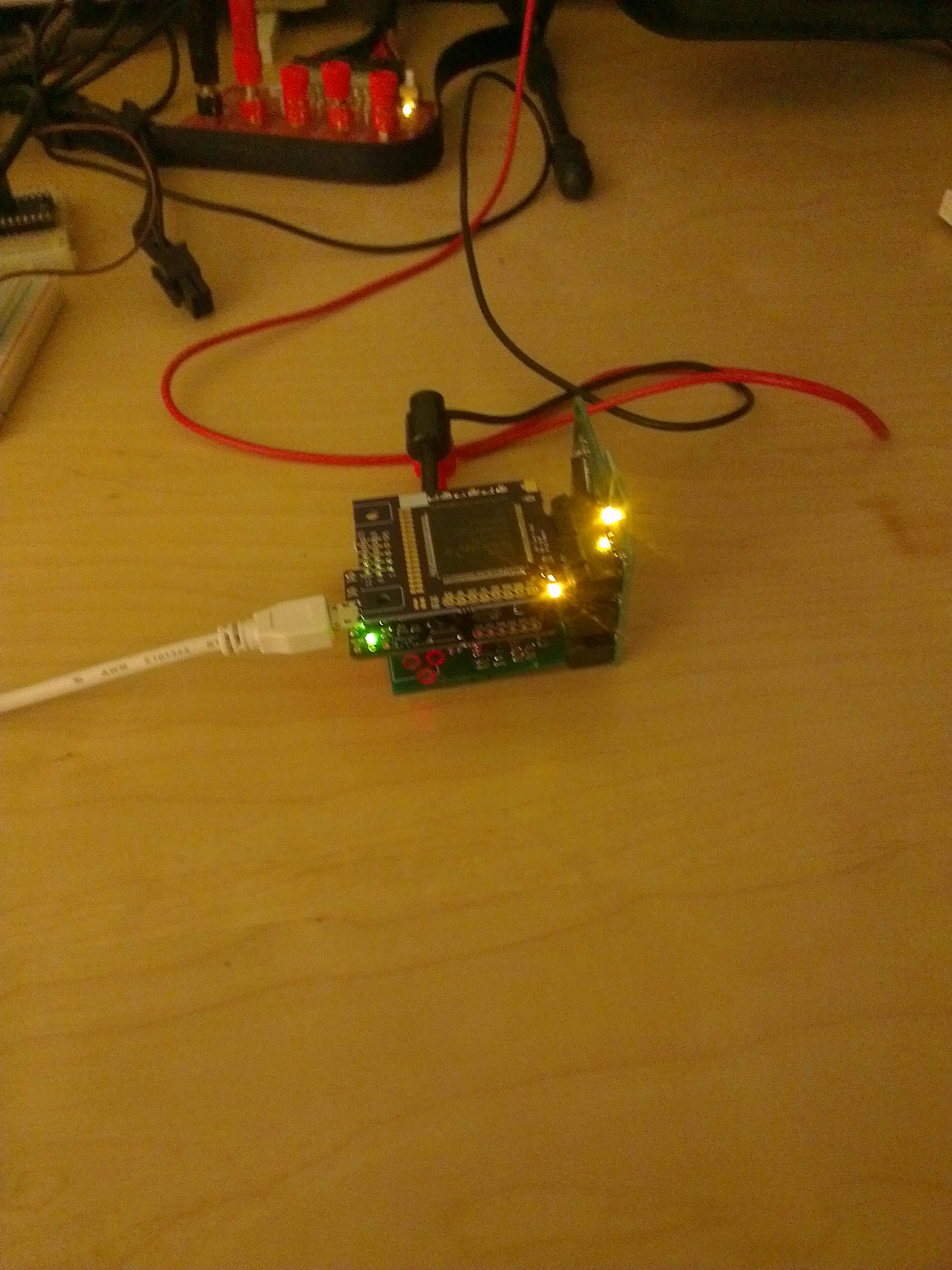
Well, I finally sort-of accomplished one of my original goals: designing and building a custom FPGA board. The reason it took a while, and somewhat separately also the reason I can’t use it very much, are both due to JTAG issues. Here’s a picture in all its low-res glory:
Without getting too much into the details, JTAG is a test-and-debug access port, which can be used for inspecting both internal chip state and external pin state. This is what I used to do my bga testing: I used JTAG to toggle the pins individually, and then read back the state of the other pins, rather than having to build a test CPLD program to do the same. Since JTAG gives you access to the devices on the board, a very common thing it is used for is configuration, and this is how I configure my FPGAs + CPLDs.
Your PC doesn’t speak JTAG, so you need some sort of converter in order to use it. Xilinx sells a $225 cable for the purpose, which is quite steep — though I imagine that if you’re paying tens of thousands for their software licenses and development boards, you don’t care too much about a couple hundred dollars for a cable. There are also open source adapters, such as the Bus Blaster; I haven’t used it but it looks legit.
Since the point of all this is education for me, there was really only one choice though: to make my own. The details aren’t super important, but it looks something like this:
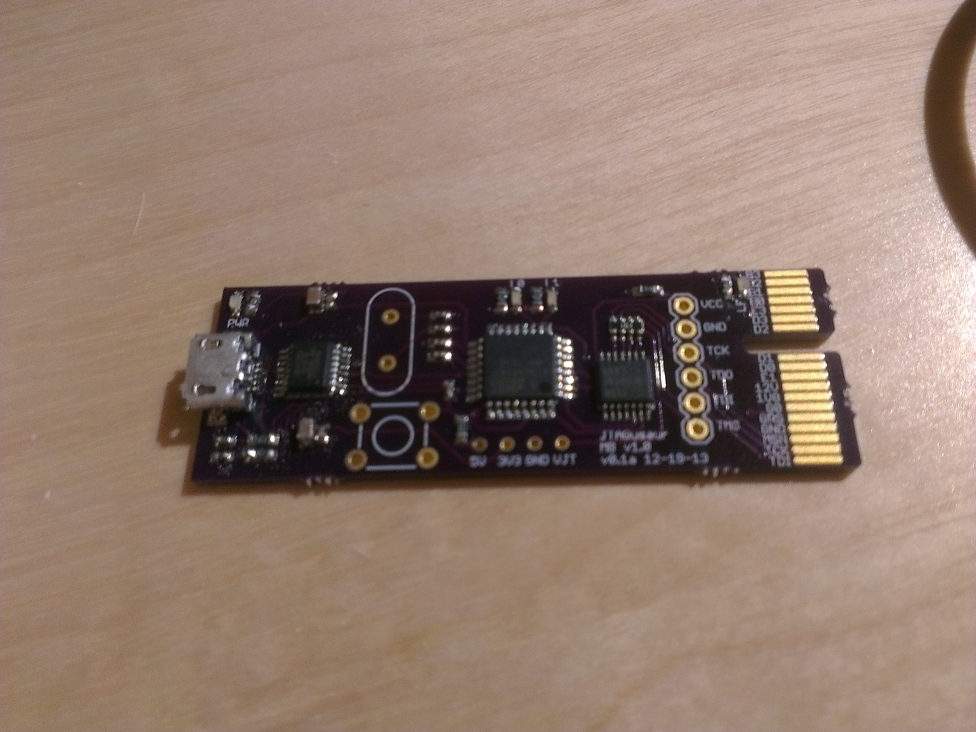
(This is actually an old version that doesn’t work at all.)
Getting the FPGA working
Most of my CPLD boards have worked without a hitch; I simply plugged in the JTAG adapter and voila, they worked and could be programmed. Either that or it was a BGA and I would see that there was a break in the JTAG chain.
I tried out my FPGA, though, and I got very odd results: it would detect a random number of devices on the chain, with random id codes. It seemed like an electrical issue, so I got out the ‘scope and saw that the TCK (JTAG clock line) would get hard-clamped at 1.5V whenever it should have gone lower. I’ve had issues like this in the past — I thought it must be some sort of diode clamping behavior, ex there was somehow an ESD diode from the 3.3V line to the TCK line due to some sort of pin assignment error.
I was only getting this behavior once I plugged in the FPGA, so I wired up the FPGA to a power source sans JTAG circuitry, and saw that the TCK line was being pulled up to 3.3V. I wanted to check how strong the pullup was — I wish there was an easier way to do this since I do it fairly often — so I connected various resistor values between TCK and GND. Using a 1k resistor pulled the TCK line down to about 0.35V, giving a pullup value of about 8kΩ. Curiously, the 0.35V value was below the 1.5V minimum I was seeing during JTAG operations, so that blew my theory about it being diode-related — clearly there was something else going on.
At this point I had a decent idea of what was happening: I had oh-so-cleverly put a bidirectional voltage translator on the JTAG adapter. I did this because the ATmega on the adapter runs at a fixed 3.3V, and having a flexibly voltage translator meant that I could in theory program JTAG chains all the way down to 1.2V. Since there are three outputs and one input from the adapter, if I used uni-directional chips I would have needed two, so instead I used a bidirectional one with automatic direction sensing.
I never really questioned how the direction sensing worked, but I realized that it was time to read about it. And for this chip, it works by weakly driving both sides at once. If one side is trying to output, it can easily overrule the weak output of the translator. The problem was that the datasheet specified that due to this, the maximum pullup strength (minimum pullup resistor value) is 50kΩ, or otherwise the sensing will get confused.
This sounded like the culprit, so I built a new version of the JTAG adapter with the translator removed and replaced with direct connections. This limits this version to 3.3V, but that’s fine since 1) I still have the other one which supports variable voltages, and 2) in practice everything of mine is 3.3V JTAG. Plugged this in, and… well, now it was correctly identifying one device, but couldn’t find the idcode. The problem was that the FPGA I’m using (a Spartan 6) uses a 6-bit instruction format instead of 8-bit like the CPLDs, and the instructions were also different, so the CPLD idcode instruction made no sense to the FPGA. I had to improve my JTAG script to test it for being both a CPLD or a FPGA, but now it seems to be able to identify it reliably.
Side-note: having pullups on the JTAG lines is a Bad Thing since some of those lines are global, such as TCK. This means that while one FPGA will have a pullup of 8kΩ, using 8 FPGAs will have a pullup of 1kΩ. What I’ll probably do instead is redesign the FPGA board to have a buffer on the global input lines, which should allow both the voltage-translator version, along with more FPGAs on a chain.
Programming the FPGA
Now that I have it connected and identified, it was time to get a basic blinky circuit on it to make sure it was working. The programming for this wasn’t too bad, aside from a mistake I made in the board design of connecting the oscillator to a non-clock-input pin, so fairly quickly I had a .bit programming file ready.
I went to go program it, and… after waiting for a minute I decided to cancel the process and add some sort of progress output to my JTAG script.
It turns out that while the CPLD JTAG configuration is composed of a large number of relatively-short JTAG sequences, the FPGA configuration is a single, 2.5Mb-long instruction. My code didn’t handle this very well — it did a lot of string concatenation and had other O(N^2) overheads, which I had to start hunting down. Eventually I got rid of most of those, set it back up, and… it took 4 minutes to program + verify. This works out to a speed of about 20Kb/s, which was fine for 80Kb CPLD configuration files, but for a 2.5Mb FPGA configuration it’s pretty bad — and this is a small FPGA.
So now it’s time to improve my JTAG programmer to work faster; I’m not sure what the performance limit should be, but I feel like I should be able to get 10x this speed, which would work out to about 80 cycles per bit. This feels somewhat aggressive once you figure in the UART overhead, but I think it should be able to get somewhere around there. This would give a programming time of 24 seconds, which still isn’t great, but it’s less than the time to generate the programming files so it’s in the realm of acceptability.
I also have a new JTAG adapter coming along that is based off a 168MHz, 32-bit ARM chip instead of a 16MHz, 8-bit AVR; I’m still working on getting that up and running (everything seems to work but I haven’t gotten the USB stack working), but that should let me make the jump to JTAG’s electrical limits, which are probably around 1MHz, for a 5-second programming time.
This FPGA is the last piece in a larger picture; I can’t wait to get it finished and talk about the whole thing.
